用於晶圓檢測的高精度白光干涉儀
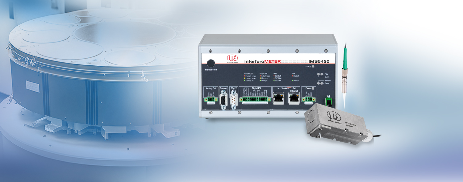
IMS5420 是一款高性能白光干涉儀,用於非接觸式測量單晶矽片的厚度。控制器配有一個經過數位化加強的發光二極體 (SLED),波長範圍為 1100 nm。這樣,只需一個測量系統就能測量未摻雜、摻雜和高摻雜單晶矽片的厚度。IMS5420 的訊號穩定性小於 1 nm。厚度測量距離為 24 毫米。
晶圓厚度的精確測量
由於矽晶片是在 1100 nm 波長範圍內的光學透明度,IMS5420 干涉儀可以精確檢測其厚度。在此波長範圍內,未摻雜矽片和摻雜的矽片都具有足夠的透明度,因此,干涉儀可以檢測到最大 1.05 mm 的晶圓厚度。可測量的氣隙(air gap)厚度甚至可達 4 mm。
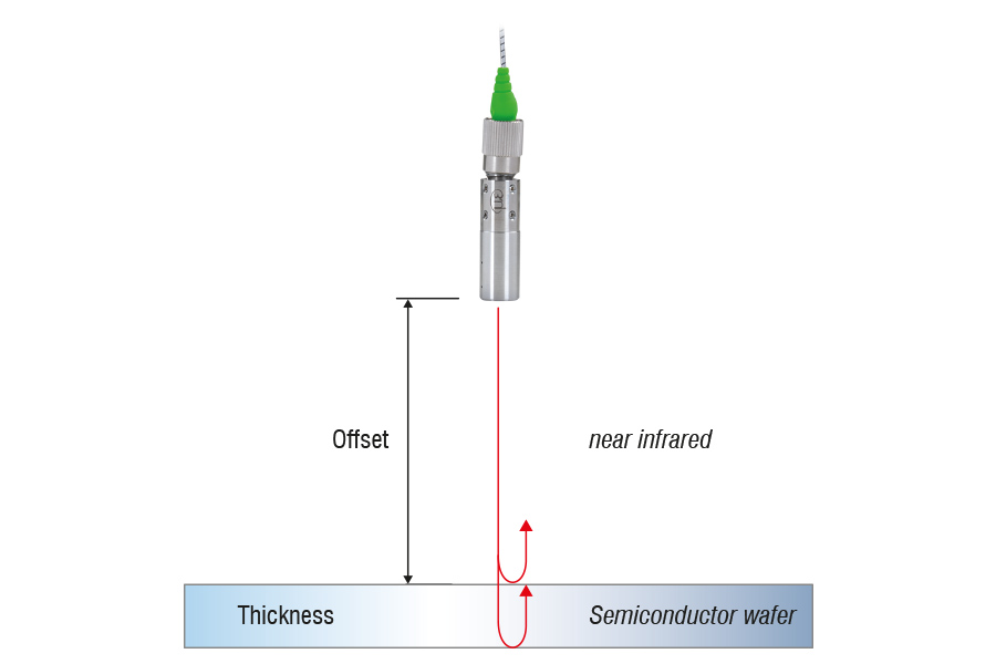
IMS5420干涉儀可實現未摻雜、摻雜及高摻雜矽晶圓的厚度測量,因而具備廣泛的應用範圍。此晶圓厚度測量系統特別適用於測量幾何厚度介於500至1050微米、摻雜濃度最高達6 m Ω cm的單晶矽晶圓。即使面對高摻雜晶圓,仍可測量高達0.8毫米的厚度。此特性源於摻雜濃度增加時晶圓透光率隨之降低的物理現象。
在研磨過程中精確測量厚度
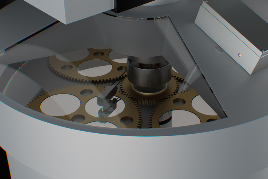
在晶圓製造過程中,晶體矽被切割成約 1 毫米的薄片。然後對薄片進行研磨,以獲得所需的厚度和表面光潔度。為了實現較高的工藝穩定性,干涉儀被用於晶圓研磨時的線上厚度測量。由於外型小巧,感測器還可以整合到狹小的安裝空間中。厚度值可用於機器控制和晶片品質控制。
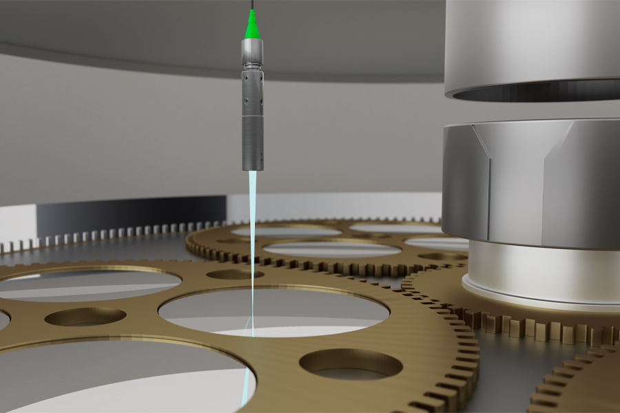
小型 IMP-NIR-TH24 感測器
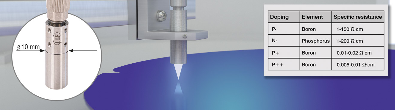
憑藉僅 10 mm 的纖細直徑以及 24 mm 的長工作距離,IMP-NIR-TH24 非常適合改裝於現有系統中。可調式安裝轉接器 (JMA) 顯著簡化了整合工作,因為即使是微小的安裝偏差或傾斜位置都能獲得可靠補償。根據需求,感測器與光纖電纜均可提供超高真空 (UHV) 設計
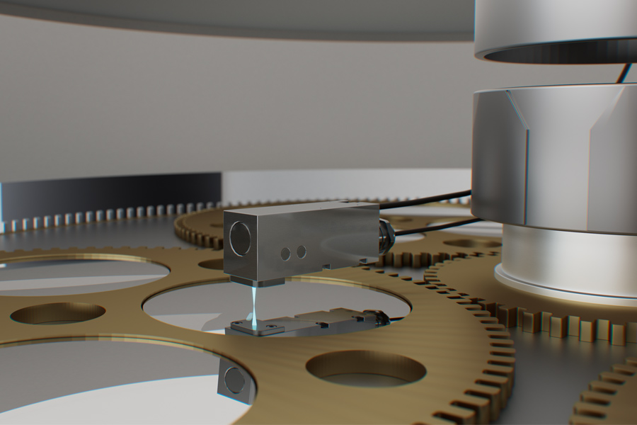
新品:堅固型 IMP-NIR-TH3/90/IP68 感測器
IMP-NIR-TH3/90/IP68 以高性能感測器擴展了產品組合,適用於特別嚴苛的安裝情況與惡劣的環境條件。此感測器以 90° 的光路設計與僅 3 mm 的短工作距離令人印象深刻 – 是極其狹窄安裝空間的理想選擇。得益於其堅固的外殼 (IP68),此感測器也適用於特別嚴苛的應用,例如漿料研磨。整合的空氣吹掃裝置可使光路持續保持無污染,從而實現永久的量測精度 – 即便是在受污染嚴重的環境中。
多種型號可滿足苛刻的量測任務
| 模型 | 工作距離/測量範圍 | 線性度 | 可測量層數 | 應用領域 |
|---|---|---|---|---|
| IMS5420-TH | 工作距離 IMP-NIR-TH24 約 24 毫米 (21 ... 27 毫米) | IMP-NIR-TH3/90/IP68 約 3 毫米 (1 ... 6 毫米) / 0.05 ... 1.05 毫米(適用於矽材料 / n=3.82),0.2 ... 4 毫米(適用於空氣,n=1) |
±100 奈米 | 1層 | 線上厚度測量,例如在研磨或拋光之後。 |
| IMS5420MP | 單層厚度誤差範圍:±100奈米 額外層厚度誤差範圍:±200奈米 |
最多5層 | 線上厚度測量,例如用於塗佈後層厚度的品質控制。 | |
| IMS5420/IP67 | 工作距離 IMP-NIR-TH24 約 24 毫米 (21 ... 27 毫米) / 0.05 ... 1.05 毫米 (適用於矽 / n=3.82),0.2 ... 4 毫米 (適用於空氣,n=1) |
±100 奈米 | 1層 | 工業化在線厚度測量技術應用於研磨與拋光工序。 |
| IMS5420/IP67MP-TH | 單層厚度誤差範圍:±100奈米 額外層厚度誤差範圍:±200奈米 |
最多5層 | 工業用線上厚度與多層測量技術於研磨與拋光製程中的應用 |
可與機器和系統整合的現代接口
控制器提供Ethernet、EtherCAT 和 RS422 等整合接口,以及額外的encoder連接、類比輸出、同步輸入和數位輸入/輸出。當使用 Micro-Epsilon 的接口模組時,還可以使用 PROFINET 和 EthernetIP。這樣就可以將干涉儀整合到所有控制的系統和生產程序中。